Superluminescent Light Emitting Diodes:
Device Fundamentals and Reliability
InPhenix, Inc.,
250 N. Mines Road, Livermore, CA 94551, USA
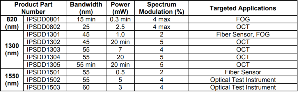
Superluminescent emitting diodes (SLEDs) have proven to be optimum light sources in optical coherence tomographs (OCTs), fiber sensor and optical coherence domain reflectometer (OCDR) applications because of their wide bandwidth and high output power. Currently, SLED devices based on GaAs/or InP material system are commercially available at 820nm, 1300nm and 1550nm windows from InPhenix. Table 1 lists InPhenix SLED product performance and their targeted applications.
Table 1 InPhenix SLED device performance and their targeted applications.
In this paper, we will review some SLED fundamentals and their proven reliability.
SLED is an edge-emitting semiconductor light source. The unique property of an SLED is its high power and low beam divergence, similar to an injection laser diode (LD), but with a broad emission spectrum and low coherence, similar to a light emitting diode (LED). SLEDs are similar in geometry to lasers but have no built-in optical feedback mechanism required by LDs for stimulated emission to achieve lasing. Main difference for SLED operations comparing with LDs are: much higher gain, much higher current density and much stronger non-uniformity of photons and carrier density distribution inside the active region. SLEDs have structural features similar to those of LEDs that suppress the lasing action by reducing the reflectivity of the facets. SLEDs are essentially highly optimized LEDs. While SLEDs operate like LEDs at low current levels, their output power increases superlinearly at high currents.
There are six key parameters used to characterize SLEDs:
(1) Output Power,
(2) Optical Gain,
(3) ASE Spectrum Bandwidth or 3dB Bandwidth,
(4) Spectrum Modulation or Ripple,
(5) Coherence Length,
(6) Coherence Function.
Every SLED has two counter-propagating beams of amplified spontaneous emission traveling along the active region. A perfect SLED would be an optimized traveling wave laser diode amplifier with zero reflection from the active channel ends. However, a perfect SLED is virtually impossible to realize due to the physical limitations of some of the manufacturing processes such as antireflection coating (AR).
Output Power and Optical Gain
The single pass Optical Gain (Gs) below saturation is determined by:
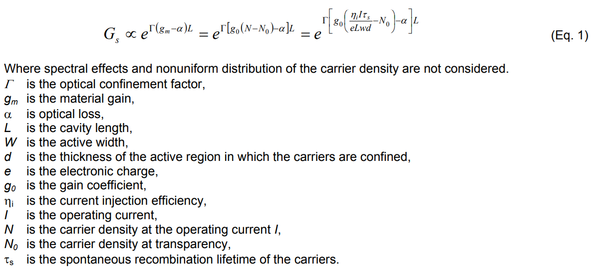
SLED Output Power has an approximate linear dependency on the optical gain and the spontaneous emission rate. A high optical gain value (between 20 and 30 dB) is usually needed to achieve high output power. Eq. (1) indicates that a high gain may be achieved using high injection current, a large optical confinement, a long cavity, a multiple quantum well (MQW) structure, or a combination of them.
Fig .1 shows typical light-current characteristics of an InPhenix 3 mW and 25mW SM fiber output SLED at
820 nm and 1300 nm windows, respectively.
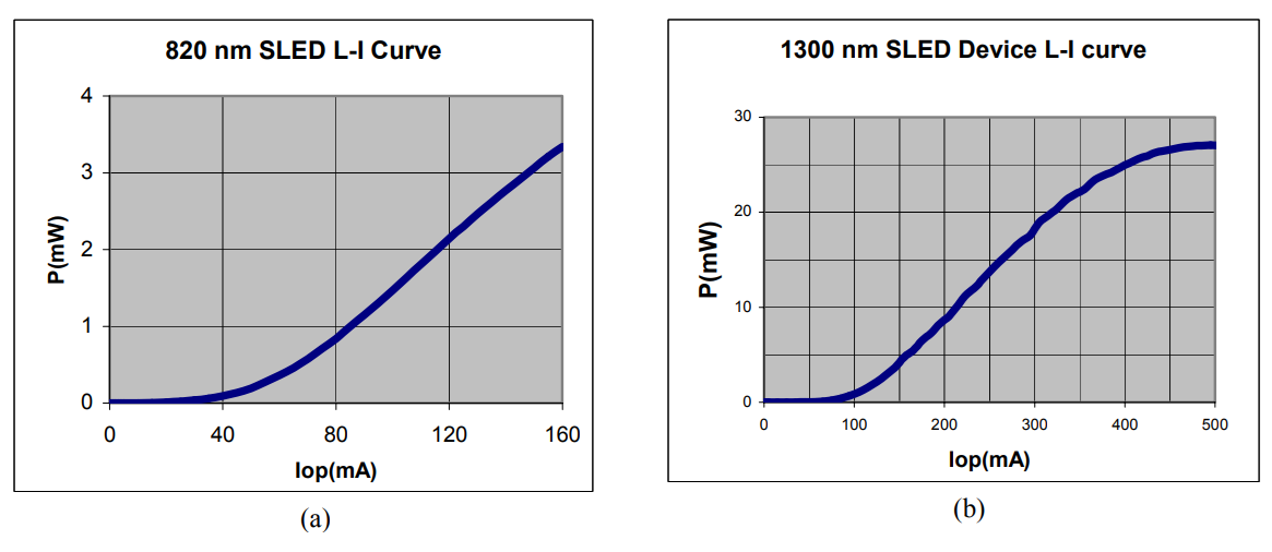
Fig. 1 L-I characteristics for InPhenix SLED devices at (a) 820 nm band (IPSDD0802) and (b) 1300 nm band (IPSDD1304)
ASE Spectrum Characteristics (Spectrum Bandwidth, Spectral Modulation or Ripple) and
Coherence Characteristics (Coherence Length, Coherence Function)
ASE spectrum characteristics can be described by:
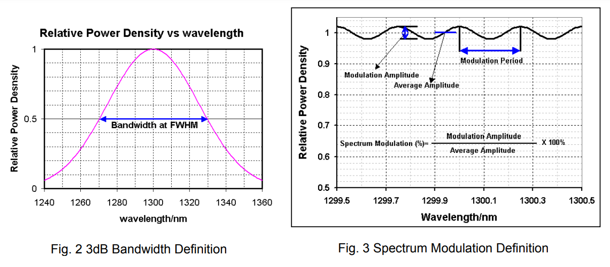
(1) 3dB Bandwidth (l3dB in unit of nm): defined as Full Width at Half Maximum (FWHM) of the ASE
spectrum as shown in Fig. 2. The range is from 10 nm to 100 nm or more.
(2) Spectral Modulation (Dm in units of % or dB): defined as peak to peak over the average amplitude at
l measured at l± dl(dl covering at least one modulation period and OSA resolution set at 0.06 nm or
better) as shown in Fig. 3. Spectrum modulation should be as low as possible (5% (0.2 dB) or less is
normal for most applications).
The bandwidth depends inversely on the optical confinement and the cavity length and it broadens as the injection current increases due to the band filling effect. In addition, SQW and MQW SLEDs will provide wider bandwidth than bulk SLEDs. The use of MQW structures at the 1550 nm band allows spectrum broadening from 50 nm to more than 100 nm as shown in Fig. 4.
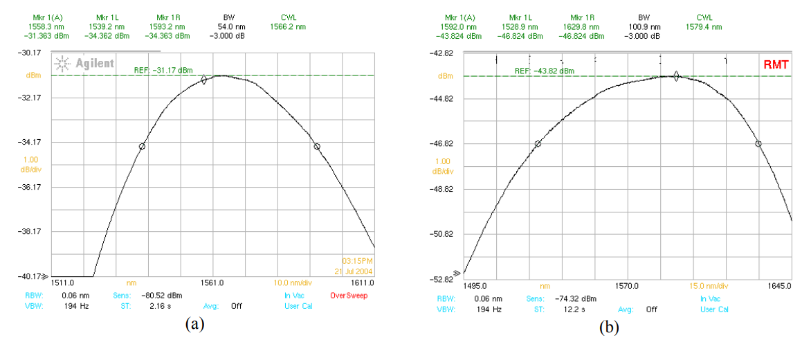
Fig. 4 1550 nm SLED bandwidth at 250 mA (Inphenix’s IPSDD1502 and IPSDD1503 Products) is about 50 nm for bulk structure (a), and 100 nm for MQW structure (b).
ASE spectrum modulation is due to the residual reflections from SLED facets and can be determined by:
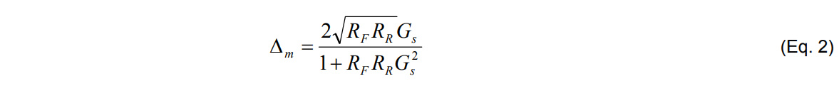
Where RF and RR is the reflectivity at the front facet and the rear facet, respectively. When Gs reaches 30 dB gain to achieve high output power, the value of RFRR must be as small as 10-10 to keep at a 2% peak to peak spectrum modulation. Several methods have been used to reduce the facet reflectivity to obtain very low spectral modulation. Examples are: Using AR-coating, unpumped absorber, short-circuited absorber, nonabsorbent window, bending waveguide, angled strip and combinations of these methods with AR-coating.
Spectrum modulation can be expressed in units of percentage (%) or decibel (dB). Fig. 5 shows the
relationship between percentage and decibel.
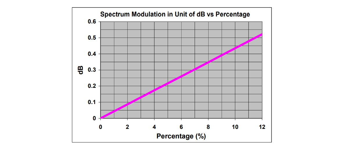
Fig. 5 Decibel versus Percentage for Spectrum Modulation
SLED coherence characteristics can be described by coherence length and coherence function. SLED Coherence Length (free space) is determined by the 3dB bandwidth of the SLED spectrum and given by: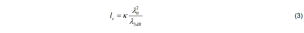
Where l0 is the central wavelength, k is a constant depending on the spectrum form-factor. In OCT literature, k ≈ 0.44 is the most common definition.
Coherence Function defines the secondary coherence sub-peak (reflectivity, dB) versus the optical path difference (or optical displacement) in mm as shown in Fig. 6. Spectrum modulation results in parasitic subpeak in coherence function at the optical path difference at a distance equal to 2neffL where neff is the effective refractive index for optical mode and L is the active length of the SLED. The intensity of secondary coherence sub-peak is determined by the integral value of the spectrum modulation across the entire spectrum. Secondary coherence sub-peak should be as low as possible.
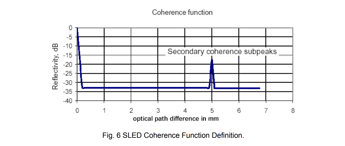
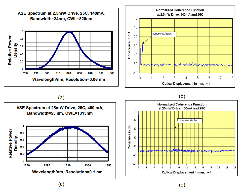
Fig. 7 ( a ) Optical spectrum and ( b ) coherence function for IPSDD0802 measured at 140 mA injection current. ( c ) Optical spectrum and ( d ) coherence function for IPSDD1304 measured at 450 mAinjection current.
As an example of the ASE spectrum and the coherence function characteristics of SLEDs, Fig. 7 shows the spectrum and coherence functions based on (1) InPhenix IPSDD0802 SLED device with 24 nm spectrum bandwidth and less than 2% (or 0.1dB) spectrum modulation, and (2) InPhenix IPSDD1304 SLED device with 55 nm spectrum bandwidth and less than 7% (or 0.3dB) spectrum modulation.
Coherence function data was quite good with a coherence measurement out to 8 mm for IPSDD0802 and more than 10 mm for IPSDD1304 with negligible artifacts as shown in Fig. 7(b) and (d), making these devices suitable for all OCDR applications.
In addition to the above six key parameters, Spatial Characteristics, Polarization, and SLED Modulations are also used to characterize SLEDs for special system design applications. Spatial Characteristics InPhenix’s SLED products are designed to be single spatial mode emission devices that allow a high coupling efficiency. SLED spatial characteristics can be described by their far field pattern. The typical far field of a SLED is shown in Table 2.
Table 2. Typical Far Field for InPhenix’s SLED Products
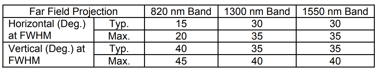
Fig. 7 shows a typical far field pattern for InPhenix IPSDD1304 with 29 x 34 degrees.
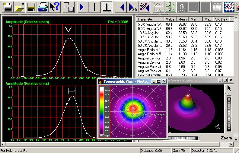
Fig. 7 Typical far field pattern for InPhenix IPSDD1304 SLED device where H represents
horizontal direction and V represents vertical direction
Polarization
SLED polarization depends strongly on the active layer structure; it can be TE (or TM) polarization dominated or polarization independent, i.e., TE/TM power ratio is close to 1. Most SLED products are TE polarized. A polarization insensitive SLED with a power difference as low as 0.2 dB between TE and TM polarizations is available from InPhenix. Fig. 8 shows an example of this type of SLED at 1300 nm wavelength windows.
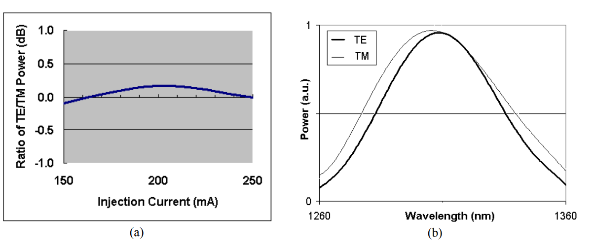
Fig. 8 (a) Optical power ratio of TE/TM versus injection current and (b) ASE spectrum for
TE and TM observed at 200 mA injection current.
SLED Modulations
SLEDs are frequently used as CW light sources and their modulation bandwidth have not been thoroughly investigated but it should be possible to directly modulate any SLED device up to 100 MHz with very little difficulty.
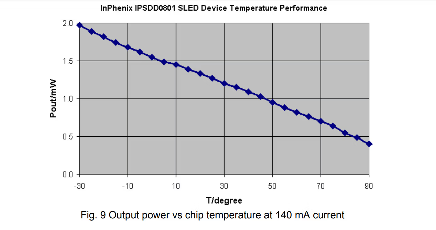
The Gain Coefficient g0(T) is temperature dependent and decays exponentially with changes in temperature. Based on Eq. (1), optical gain depends strongly on temperature, therefore SLED power is strongly dependent on temperature too. Fig. 9 shows an example for power dependence on temperature from –30 C to +90 C using an InPhenix IPSDD0801 SLED device.
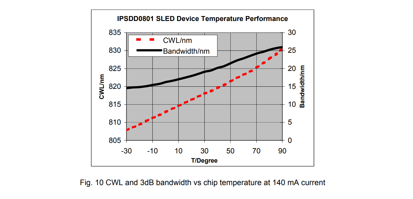
SLED central wavelength (CWL) and spectrum bandwidth also change with changes in the ambient temperature as shown in Fig. 10 using an InPhenix IPSDD0801 SLED device.
It should be pointed out that increasing SLED current should not be used for compensation of power decreasing with temperature since this will reduce SLED lifetime significantly due to high carrier density. SLED temperature performance also strongly depends on the driving mode such as constant current or constant power, active layer structure such as bulk or MQW, and a number of other parameters such as cavity length and/or operating wavelength window. Customers are encouraged to contact us for the specific details of each particular type of InPhenix SLED product.
Physical processes inside the SLED are governed by the carrier injection and the photon generation processes when the SLED temperature is regulated by a TEC. The Carrier Injection process can be described by the rate equations. The photon generation process can be described by the traveling wave equation derived from the basic Maxwell equations. Photon density for the forward and backward propagating waves can be determined by the boundary conditions of the SLED related to the AR coating and any feedback from the optical interface.
The carrier density and distribution inside a SLED is the key to understanding the performance changes caused by optical feedback. Carrier density and distribution is directly related to the forward and
backward light intensities, which are determined by the reflectivity of both facets and the fluctuation of the feedback light into the SLED. Eq. (2) shows that SLED spectrum modulation is highly sensitive to external optical feedback (optical feedback can be equivalent to the effective facet reflectivity) especially for high optical gain devices. Any returned light will be amplified in the SLED active region and will cause redistribution of the carrier density inside the SLED. This will cause performance changes such as increased spectrum modulation, central and peak wavelength shifts, narrowing the bandwidth, the output power stability, and degradation of the device’s reliability and service life.
To minimize the performance changes due to the external feedback into the SLED, APC connector is recommended to use, especially for powerful SLED device.
A SLED’s long term operational stability and reliability can be improved by optimizing the design, improving the crystal growth, optimizing manufacturing processes, using better heat sinks, eliminating mechanical stress, and developing more efficient facet passivation technology and bonding methods coupled with proper analysis of the various factors causing SLED degradation.
SLED intrinsic degradation mechanisms can be separated into four categories:
(1) Defect formation in the inner region of the chip,
(2) AR coating quality,
(3) Facet damage due to oxidation that affects facet reflectivity,
(4) Catastrophic mirror damage at high power densities.
An LDs life is dependent on the driving current density. A SLEDs operational life may be less than that of a similar LD in terms of output power due to (1) the use of considerably higher current to achieve the same output power and, (2) non-uniform carrier distribution inside the SLED active region may speed up and overstress the device at the higher driving current densities.
SLED life is also determined by several other factors. These are design, materials (such as AlGaAs/GaAs or InGaAsP/InP), manufacturing process quality, the operation current density, and how the SLED is used. Like LDs, SLEDs are very sensitive to electrostatic discharges, overheating, overdriving by spikes/surges, and negative voltages. Therefore, the stability of the temperature and driving current are the key factor to extending a SLEDs extrinsic lifetime. In addition, external optical feedback should be avoided or minimized since it may easily result in fatal SLED degradation, especially for powerful SLEDs.
InPhenix SLEDs are designed and manufactured for long life, operational stability and high reliability. Our products have been successfully tested to the following standards:
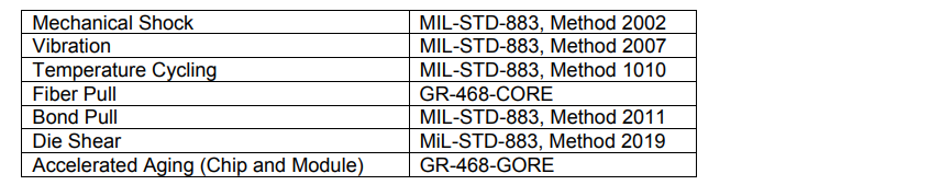
InPhenix can provide DIL/14-pin, BUT/14-pin and BUT/8-pin SLED devices with SMF/PM pigtails over with a wavelength range from 780 nm to 1650 nm. All products are thoroughly tested to be reliable over the long term. Our quality assurance and testing programs have been carefully implemented to guarantee the highest fabrication and manufacturing standards and proven reliability for our customers.